|
|
NEXCOM Networking and Communication: Powerful Enterprise Networking Solution for Cybersecurity Application
NEXCOM Network and Communication Solutions Busines...
NEXCOM Networking and Communication: Powerful Enterprise Networking Solution for Cybersecurity Application
|
|
|
NEXCOM NSA 7160R Shaping Future Networks for Edge AI
Discover the cutting-edge capabilities of the NEXC...
NEXCOM NSA 7160R Shaping Future Networks for Edge AI
|
Ultra High-Speed Signal Design, its Innovation and Application to High-end Network Platforms
 With the advent of 5G era, a revolution of telecommunication is taking place in a mega scale never seen before. Huge data volume, along with its required data streaming capacity, has driven to the birth of new generation high-speed, broad-band network equipment. High-speed signal integrity emerges as one of the major challenges for designing high speed network platforms—how insertion loss, VIA effect, and SSN (Synchronized Switching Noise) of high speed printed circuit board can be minimized and controlled, is the key to perfecting the performance of telecommunication equipment. In light of such necessity, NEXCOM, ITRI (Industrial Technology Research Institute), FHT (First Hi-Tec), and TUC (Taiwan Union Technology Corp.) have partnered up to co-develop new technology to overcome such challenge of high-speed signaling.
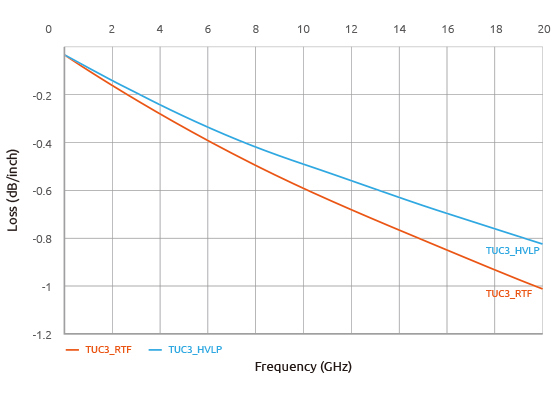
Figure 1. TUC3 correlation of signal speed and insertion loss.
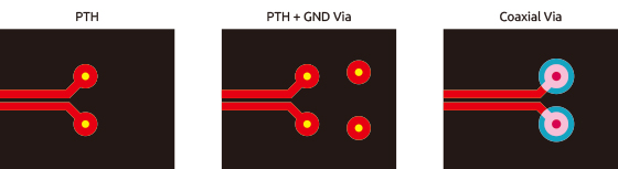
This 4-party alliance has introduced a new type of ‘Ultra Low Loss’ material called TUC3, whereas the Insertion loss can reach as minimal as -0.57dB/inch @25Gbps (Figure 1). Another brainchild, named Coaxial VIA (as shown in Figure 2 Coaxial VIA Architecture), is an innovative technology that outperforms in signal simulation in which Sdd21 index reads -0.2dB@8GHz, -0.3dB@12.5GHz and -1.2dB@28GHz ,respectively, while the same index reads 0.3dB@8GHz, 0.5dB@12.5GHz and 1.6dB@28GHz through traditional PTH VIA (Figure 3). In the comparison chart of Coaxial VIA vs PTH (Plating Through Hole) or PTH+ GND VIA, we see the higher the speed transmission, the greater difference in performance and signal integrity (Table 1). It leads us to adopt Coaxial VIA in PCB layout to maintain signal integrity when it comes to high speed signal in general.
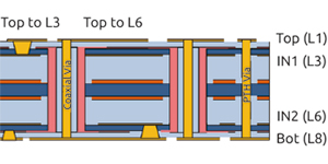
Figure 2. Coaxial VIA stack-up.
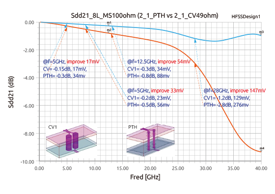
Figure 3. Simulation of Coaxial VIA vs PTH@Sdd21 across different speeds.
|
Simulation Improvement (mV)
|
Signal Measurement + Improvement (mv)
|
|||||||||
|
CV1
|
PTH
|
Intel GND Via
|
Coaxial Via 1
|
Coaxial Via 2
|
Coaxial Via 3
|
|||||
|
@10Gbps
|
17
|
381
|
396
|
15
|
397
|
16
|
400
|
19
|
402
|
21
|
|
@16Gbps
|
33
|
336
|
352
|
16
|
355
|
19
|
356
|
20
|
356
|
20
|
|
@25Gbps
|
54
|
199
|
222
|
23
|
269
|
70
|
281
|
82
|
284
|
85
|
Table 1. Signal measurement of types of VIA @ different speeds.
The third innovation brought to the world by the team is the embedded capacitor (in red path) layered in PCB FAB as shown in Figure 4, which, if compared with current mainstream SMD type of capacitor (in green path), reduces the circuitry traces by 50% and as a result greatly enhances the signal integrity since it cuts down much of the SSN generated by high speed IC chip (such as Mellanox ConnectX-5, etc). (Figure 5) demonstrates the PCB FAB with embedded capacitors whose capacity is 0.01uF @8GHz, resistance @6 Ohm.
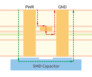
Figure 4. Trace length-embedded capacitor (red) vs SMD capacitor (green).
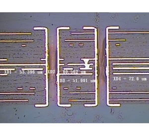
Figure 5. Cross Section, PCB FAB with embedded capacitors.
NEXCOM has developed a 100G LAN module showcasing the three innovation put together by the alliance (Figure 6). The LAN module supports 100G controller in 2 x100G QSFP28. Port 0 is designed following the 100G IC-maker’s design guideline, using PTH+GMD VIA and high speed signal circuitry compliant to 3” length limitation; Meanwhile, the design of Port 1 is built on above 3 innovative technology, thus allowing the high speed signal to extend the length up to 14” (Figure 7). During the validation of IEEE conformance test, Port 1 QSFP28 of this 100G LAN module meets perfectly IEEE 802.3bm requirements as shown in the Eye Diagram (Figure. 8).
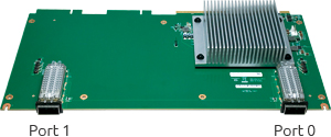
Figure 6. 100G LAN module snapshot.
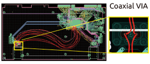
Figure 7. 100G LAN module PCB layout.
|
npoc240
|
|
Port No.
|
Eye Height
(95mV) |
Eye width
(17.84ps) |
Jitter
|
Pass/Fail
|
|
TUC-3, 14inch
Port 0 (14") |
Sample A
|
TX1
|
142
|
20
|
18.7
|
PASS
|
|
TX2
|
117
|
19.6
|
18.6
|
PASS
|
||
|
TX3
|
142.6
|
22.1
|
17.3
|
PASS
|
||
|
TX4
|
129.8
|
21
|
17.3
|
PASS
|
||
|
Sample B
|
TX1
|
176.6
|
18.4 |
18.1
|
PASS
|
|
|
TX2
|
140.4
|
20.7
|
20.1
|
PASS
|
||
|
TX3
|
189.4
|
22.4
|
16.8
|
PASS
|
||
|
TX4
|
175.5
|
20.5
|
16.7
|
PASS
|
||
|
Sample C
|
TX1
|
158.1
|
22.1
|
15.5 |
PASS
|
|
|
TX2
|
155.3
|
18.5
|
19.9
|
PASS
|
||
|
TX3
|
170.2
|
22.1
|
17.7
|
PASS
|
||
|
TX4
|
136.2
|
18.1
|
16.7
|
PASS
|
||
|
Average
|
153.6
|
20.4
|
17.8
|
PASS
|
||
Figure 8. Readings of eye diagram, port 1, 100G LAN module.
This card, when installed in Intel Purley Platform NEXCOM NSA 7146, and runs under NEXCOM’s own DPDK, we witness impressive figures of throughput (Table 2). We achieve this without any addition of repeaters, re-timers and any other active component to safeguard its signal integrity and maintain the desired performance. This 100G LAN module marks a milestone, a true breakthrough in high speed signal design.
|
Frame Size
|
Throughput
|
% 100gb/s
|
|
512B
|
1,330,474,624/1,255,701,950
|
94.38
|
|
1024B
|
718,385,872/718,385,872
|
100
|
|
1280B
|
576,907,231/576,907,231
|
100
|
|
1518B
|
487,646,294/487,646,294
|
100
|
Table 2. Throughput, port 1, 100G LAN module.
![]()
- Related Links:
- NEXCOM Brings Expanded Edge, Security, and Quantum-Resistant Innovations to MWC Barcelona 2026
- NEXCOM Drives Edge AI, Dual 5G, and OT Security Innovation at CommunicAsia 2025
- Browse Other News:
- AMR Robotics Guide: Technology, Industrial Applications, and Benefits
- NEXCOM (8234) Forges Strategic Collaboration with Qualcomm to Accelerate Embodied AI Robotics Development at COMPUTEX
- All White Papers News